Surface Defect Inspection Systems
Surface Defect Inspection Systems
Candela® surface defect inspection systems detect and classify a wide range of critical defects on compound semiconductor substrates. Surface defect inspection substrates include GaN, GaAs, InP, sapphire, SiC, etc. and hard disk drives, with high sensitivity at production throughputs.
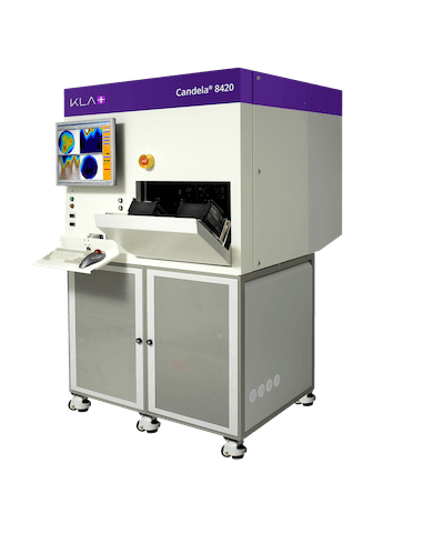
Candela® 8420 Surface Defect Inspection System
Optical Surface Analyzer (OSA) for tool and process monitoring, through surface defect detection and classification of surface defects including particle, stains, scratches and macro epi defects for photonics, LED, communications and other compound semiconductor applications.
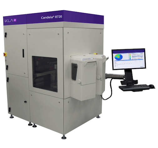
Candela® 8720 Surface Defect Inspection System
High sensitivity wafer inspection tool, integrating surface defect detection and photoluminescence metrology for GaN applications in HBLED, MicroLED, VCSELs, LiDAR, IoT, 5G and other high-end compound semiconductor applications.
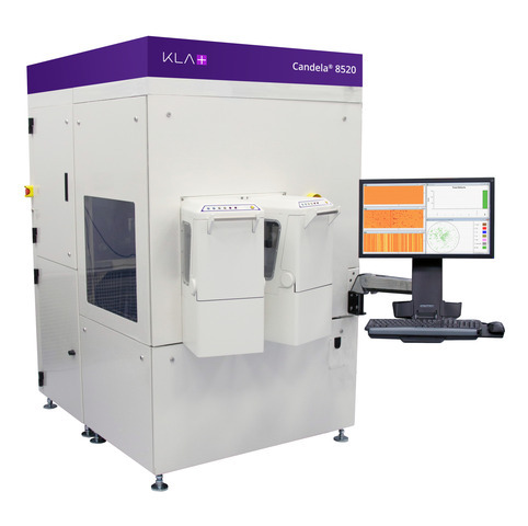
Candela® 8520 Surface Defect Inspection System
High sensitivity, high throughput wafer inspection tool, with integrated surface scattering and photoluminescence technology for defect detection and classification of topographic and crystallographic defects on SiC and GaN based power devices.
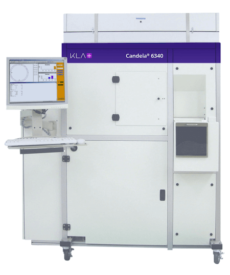
Candela® 6300 Series Optical Surface Analyzer Systems
Laser based surface inspection system for hard disk drive (HDD) substrates featuring innovative Optical Surface Analysis (OSA) technology that measures full disk surface topography, micro-roughness and waviness, and inspects the wafer surface for defects. The automated model, Candela 6340, includes disk cassette-to-cassette handling.
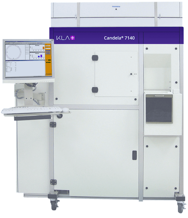
Candela® 7100 Series Defect Detection and Classification System
Laser based surface inspection system for high sensitivity surface defect inspection of hard disk drive (HDD) substrates and media, featuring multiple optical paths for classification of submicron pits and particles. The automated model, Candela 7140, includes disk cassette-to-cassette handling.
Looking for wafer defect inspection and review systems for semiconductor chip and wafer manufacturing?
View MoreTechnical Literature
Browse application notes and technical papers from KLA Instruments Application Engineers and customers, covering a variety of use cases for KLA Instruments products.
Timeline of Innovation
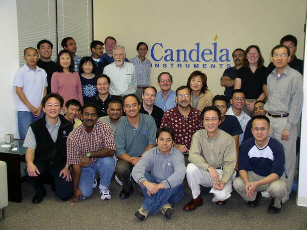
Since the launch of the Candela Optical Surface Analyzer (OSA) in 1997, our technical experts have continued to introduce key innovations in defect sensitivity and classification for the compound semiconductor and data storage markets. Our inspection technology provides performance improvements with each new product release, including our industry-first, award-winning ability to combine high-speed surface defect detection and photoluminescence metrology on a single platform. Learn more about the rich history of innovation of our Candela defect inspectors.
Receive the latest KLA Instruments news, papers, events, and more
Follow KLA Instruments
Follow KLA Instruments to engage with our experts and learn about our tool applications.
Learn how our products can help you.
Explore More Solutions
Instruments
For industry experts, academics and other innovators, KLA Instruments delivers trusted metrology and defect inspection solutions that provide measurements that enable the world’s breakthrough technologies.
Sheet Resistance Measurement
The Filmetrics® sheet resistance mapping instruments have been developed based on over 45 years of resistance measurement innovation and technical expertise.
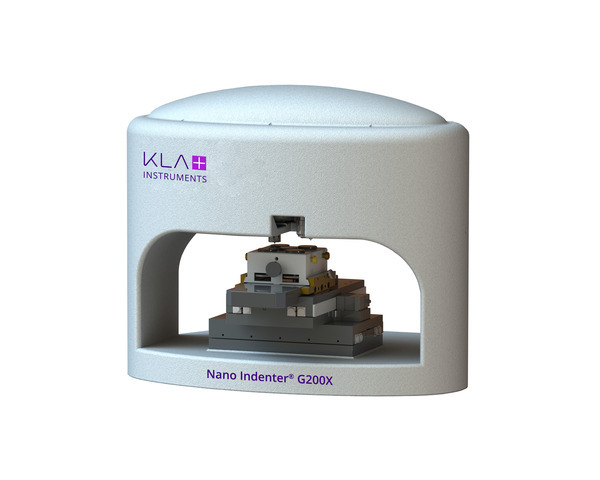
Nanoindenters
The KLA Instruments nanoindenter portfolio provides precise, reliable and repeatable testing to characterize static and dynamic mechanical properties of materials, under a wide range of test conditions.
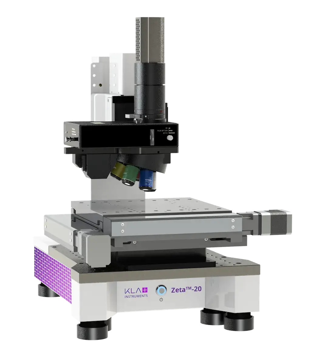
Optical Profilers
The Profilm3D® and Zeta™ optical profilometers offer fast, non-contact solutions for 3D step height, roughness, and other surface topography measurements, leveraging interferometer and ZDot™ measurement techniques.
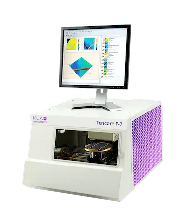
Stylus Profilers
The Alpha-Step®, Tencor® P-series and HRP® stylus profilometers enable high-precision, 2D and 3D surface metrology. The stylus profilers measure step height, roughness, bow and stress with industry-leading stability and reliability for your R&D and production metrology requirements.
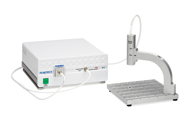
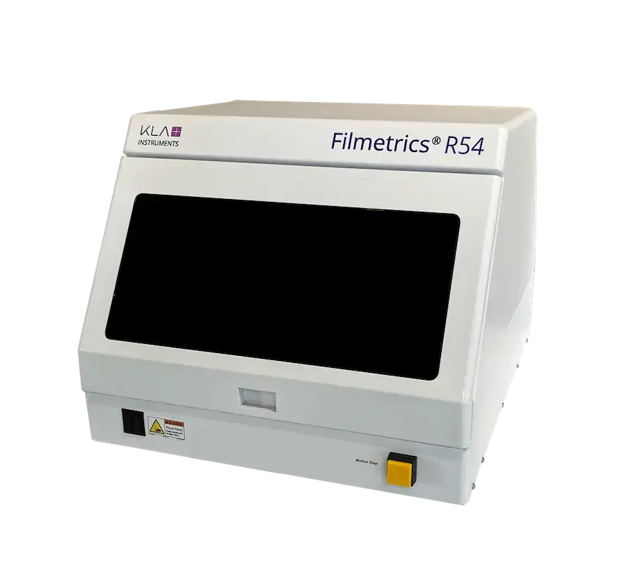
Thin-Film Thickness Reflectometers
The Filmetrics® thin-film reflectometers provide thickness and refractive index measurements of transparent films in seconds, with industry-leading precision.