Candela® Instruments Innovation History
The first Candela Instruments optical surface analyzer (OSA) is introduced to characterize surface defects for the hard disk drive (HDD) industry.
The Candela optical surface analyzer (OSA) is a multi-channel laser-based defect inspection system for R&D and process monitoring, designed specifically for the HDD industry. The new inspection system characterizes surface defects such as particles and scratches on disk substrates and finished media, providing significant advantages over traditional manual visual inspection.
Learn more about our latest offerings in this product series:
The TS 2100 extends hard disk drive (HDD) tribology capability by adding magnetic imaging and measurement of the carbon layer and lubricant layer. The TS 2100 also includes improvements to measurement sensitivity, speed and resolution.
The OSA 5100 and 5120 are the fifth generation Candela OSA systems, adding disk surface topography measurement. The OSA 5120 is equipped with an automated disk cassette-to-cassette handler to deliver defect detection and classification capability to high volume HDD manufacturing.
The new Candela CS1 and CS2 systems address compound semiconductor wafer inspection applications, providing the unique capability to inspect both transparent and opaque wafers for detection and classification of particles and other process-related defects.
The Candela OSA 6100 and 6120 series systems introduce X-Beam channel technology, adding radial illumination to the existing circumferential illumination design, plus advanced collection optics that extend defect sensitivity down to 80nm. This multi-channel system simultaneously detects and classifies defects such as particles, pits and stains; characterizes lubricant thickness, and uses the Kerr Effect to characterize magnetic imaging.
KLA-Tencor acquires Candela Instruments, the leading supplier for laser-based surface inspection systems optimized for the data storage industry, measuring metal and glass substrates, plus finished media.
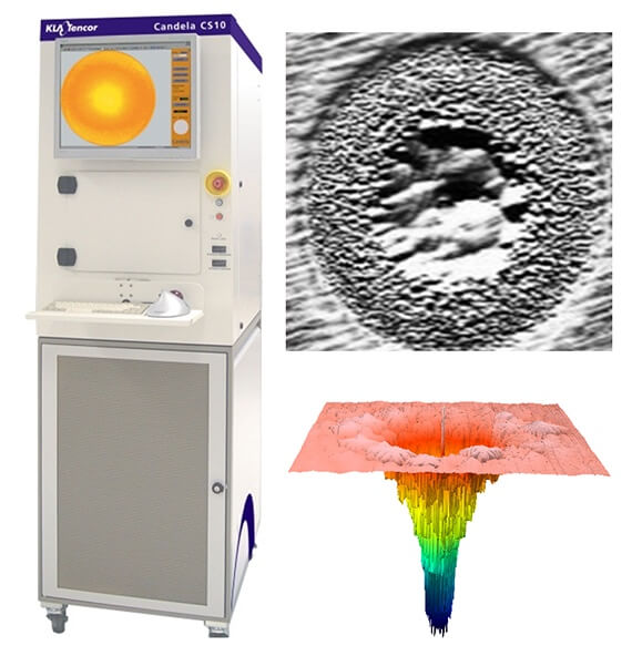
The Candela CS10 and CS20 system are released for inspection of defects on power devices, high brightness LEDs, and other compound semiconductor devices.
The new Candela CS10 and CS20 systems are designed to replace manual visual inspection of compound semiconductor wafers with automated defect inspection. These second-generation Candela CS systems also introduce a new defect location trace-back feature to facilitate offline defect review. The CS10 and CS20 systems provide advanced surface analysis for detection and classification of a variety of defects for power devices, high brightness LEDs, specialty coatings on glass, CMOS image sensors and LCoS displays.
Learn more about our latest offerings in this product series:
The Candela 6300 and 6320 series systems include design improvements that deliver the wide spatial bandwidth and low noise floor required for accurate measurement of surface roughness and waviness measurements of HDD substrates.
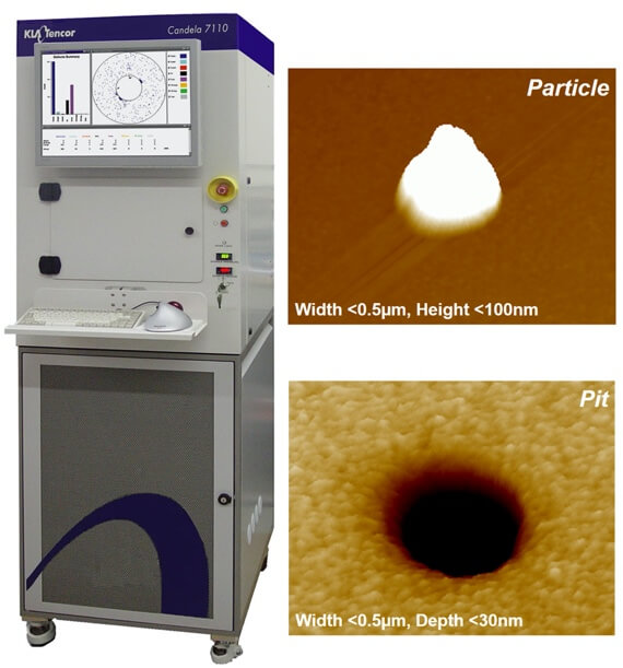
The Candela 7100 and 7120 series systems include the unique capability to discriminate submicron pits from particles on HDD metal substrates.
The Candela 7100 and 7120 introduce two new scatter channels to enhance defect detection and classification capability on hard disk drive substrates. The new stealth scatter channel improves capture of submicron-height defects by suppressing background noise. Comparing signals from the new normal scatter, new stealth scatter, and existing oblique scatter channels enables discrimination of submicron pits from particles, an important innovation because particles may be cleanable, while pits are not. In high sensitivity mode, defect sensitivity is enhanced to 40nm on metal substrates.
Learn more about our latest offerings in this product series:

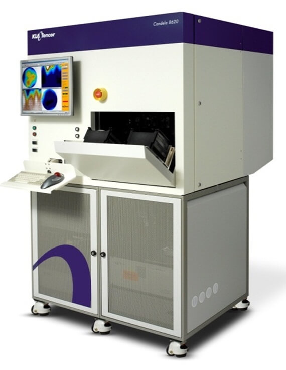
The Candela 8600 and 8620 series release with integration of a new photoluminescence channel for capturing GaN defects that are not visible to typical scatter channels.
The Candela 8620 systems are designed for substrate wafer quality inspection and gallium nitride (GaN) epi process control in the LED industry. This new inspection platform integrates proven Candela inspection techniques with a new photoluminescence mode to capture both surface defects and multiple quantum well (MQW) defects. In addition, the 8600 series systems provide the unique capability to detect cracks and differentiate submicron pits from particles on LED wafers.
Learn more about our latest offerings in this product series:
The Candela 8720 system delivers a 4x improvement in positioning accuracy over its predecessor, the Candela 8620. It features an improved handler module, and enhanced defect detection and classification on III-V (GaN, GaAs, InP) epitaxial films for LED, communications (RF, 5G, VCSEL, Photonics) and other high-end compound semiconductor applications.
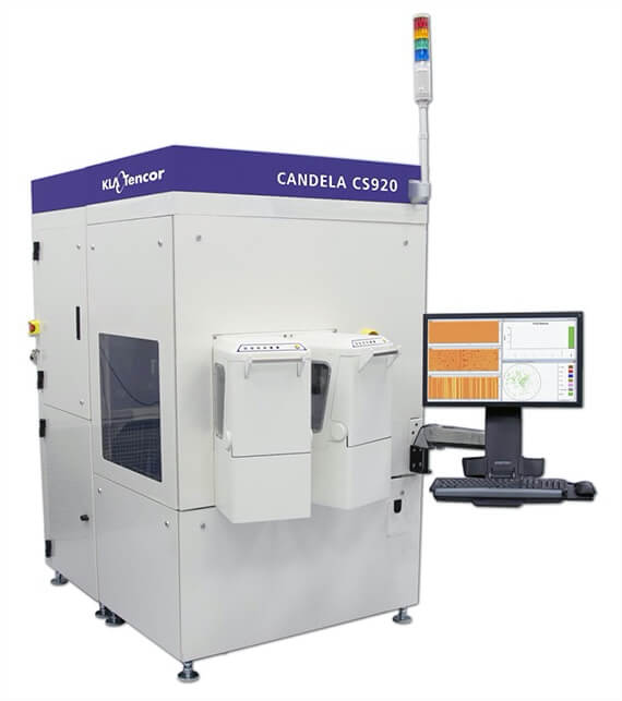
The Candela CS920 releases with a UV laser designed for high sensitivity to defects on Silicon Carbide substrates and epitaxy layers.
The Candela CS920 systems are the power device industry’s first integrated surface and photoluminescence defect detection systems for Silicon Carbide (SiC) wafers. The Candela CS920 platform is equipped with a ultra-violet (UV) laser that enables complete back-side elimination on visually transparent SiC substrates and high sensitivity to nanometer-level scratches on SiC substrates. These scratches can impact epitaxy yield. The new system design enables detection and classification of SiC epitaxy layer surface defects including surface triangles, carrots, and down fall, plus crystal defects including stacking faults and basal plane dislocations (BPD).
Learn more about our latest tool offerings in this product series:
The Candela 8420 systems feature hardware and software design improvements that boost throughput by up to 70% over the CS20. The 8420 series supports process monitoring, tool monitoring and tool qualification.
Zeta Instruments joins the KLA Instruments group, expanding KLA’s unpatterned wafer inspection product line, adding line scan technology on the ZetaScan platform. The ZetaScan supports R&D and production environments for detection and classification of defects on square or round GaAs, glass and sapphire wafers for solar, PV and display applications.
The Candela 8520 system retains the innovative technology of the Candela CS920 while boosting throughput by up to 2.3X. The 8520 also introduces the capability to detect stacking faults on SiC substrates and delivers improved detection and classification of basal plane dislocations on SiC epitaxial wafers.