Enjoy the previously unreleased interviews with KLA’s engineering teams below! The original post follows.
Today, KLA Corporation announced the launch of three new semiconductor packaging systems to drive innovation and improve yield and quality. As chip scaling has slowed, advances in packaging technology have become instrumental in driving device performance. The constant, industry-wide demand for improvements in performance, power consumption and cost has driven increasingly diverse and complex packaging designs that become smaller and more densely packed with every generation. For example, heterogeneous integration, where multiple chips are included in the same package, has become increasingly common. These increases in complexity have caused the value of the packaged chip to grow substantially, along with electronics manufacturers’ expectations for quality and reliability. To meet these expectations, packaging manufacturers have demanded more sensitive and cost-effective inspection, metrology and data analysis, and more accurate identification of bad parts. Our engineering teams have developed the Kronos™ 1190 wafer-level packaging inspection system, the ICOS™ F160XP die sorting and inspection system and the next generation of the ICOS™ T3/T7 Series of packaged integrated circuit (IC) component inspection and metrology systems to serve the electronics industry’s growing needs for production-worthy defect detection for a wide variety of packaging types.
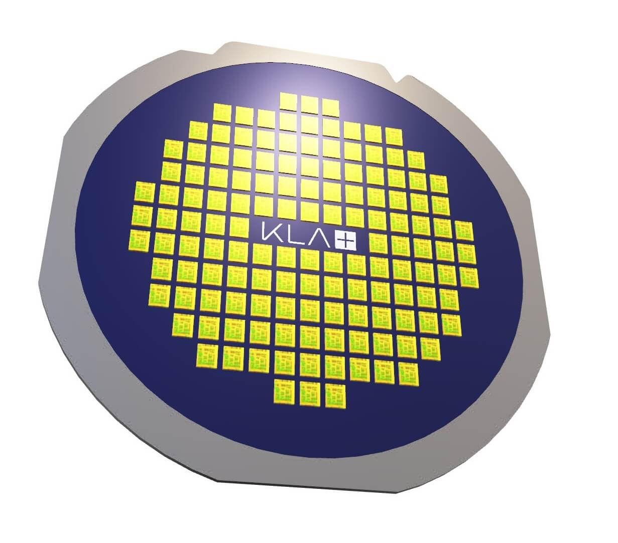
The Kronos™ 1190 system provides sensitive defect inspection, helping chip manufacturers to quickly detect, resolve and monitor excursions to provide greater control of quality during wafer-level packaging.
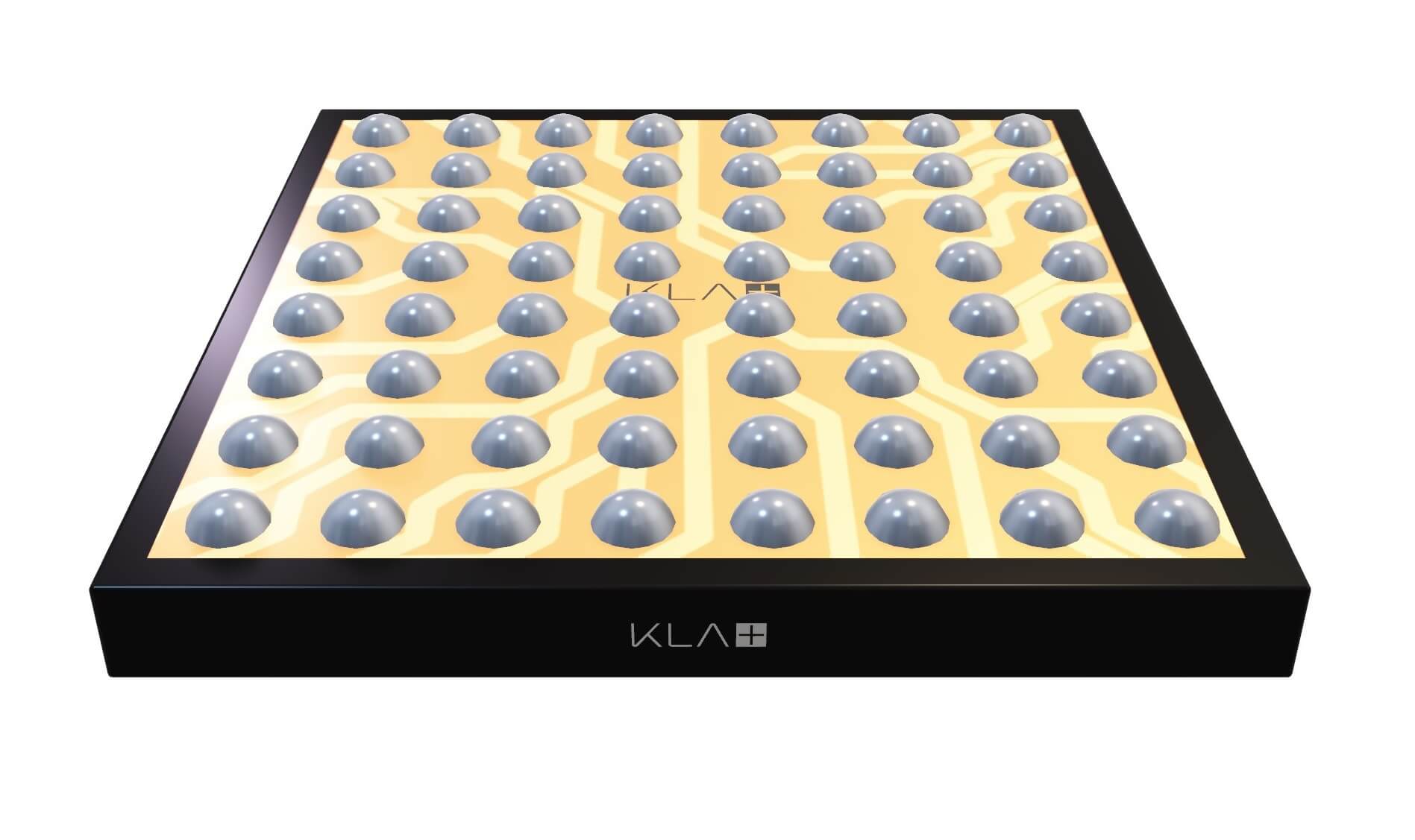
The ICOS™ F160XP system provides accurate, fast inspection before die assembly to help engineers quickly identify any issues like cracking during the dicing process of wafer-level packages to ensure higher outgoing quality.
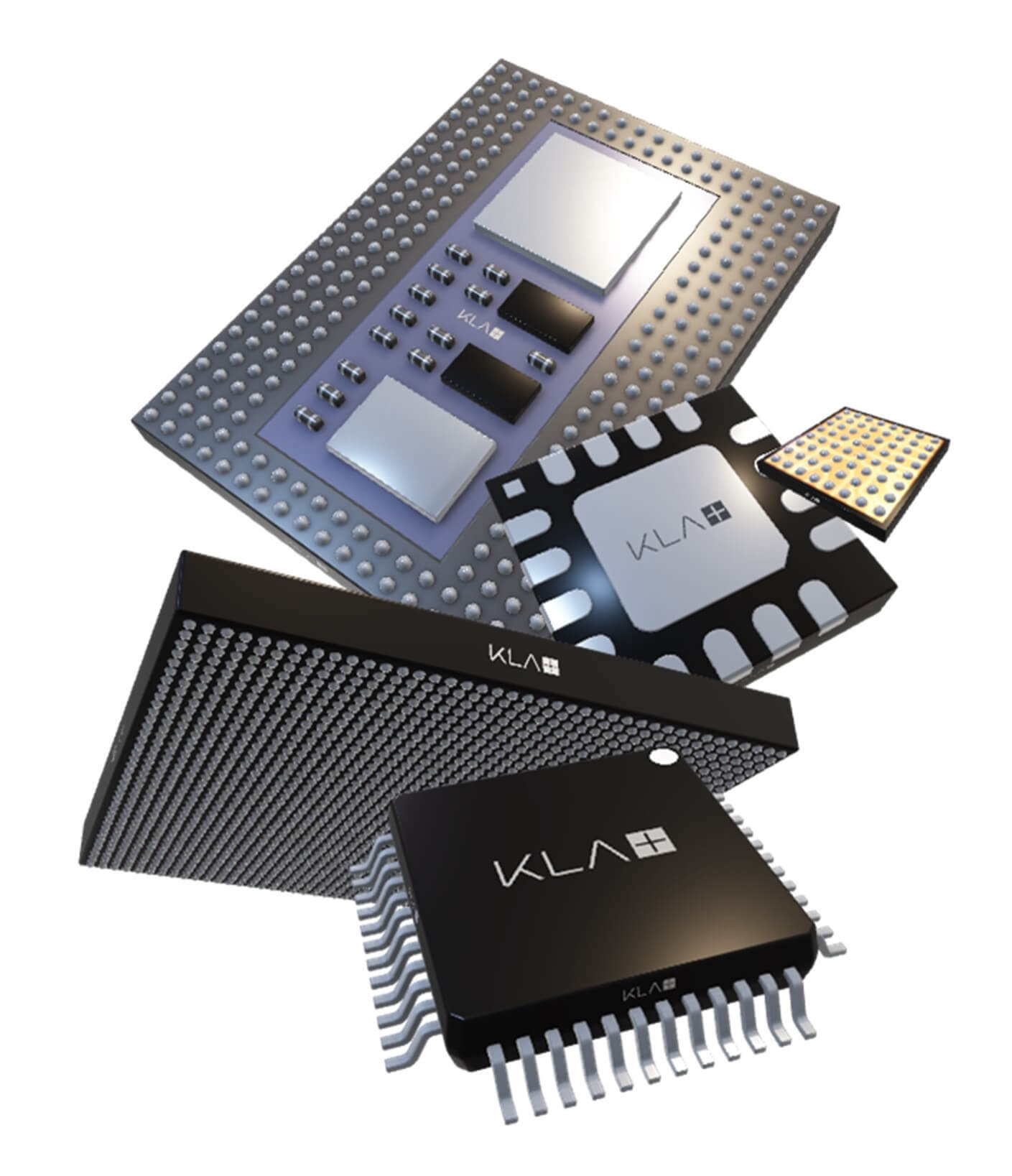
The ICOS™ T3/T7 Series provides sensitivity to defects and accurate 3D metrology for assembled packages, allowing packaging manufacturers to accurately sort good components from bad and improve yield.
Read the News! See the latest press release here.
Want to learn more about KLA’s packaging portfolio? See our packaging manufacturing portfolio here.
Follow Us