Product Description
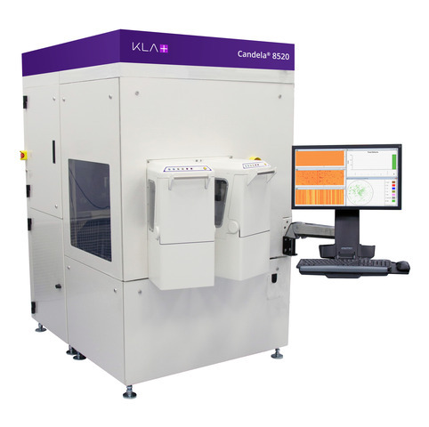
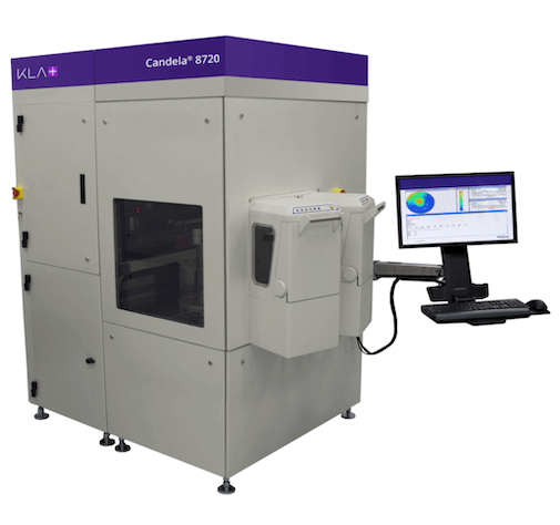
The Candela 8420 wafer inspection system provides surface analysis including surface defect and particle detection on opaque, translucent and transparent wafers including glass, single side polished (SSP) sapphire, double side polished (DSP) sapphire; sliplines; Gallium Arsenide (GaAs) and Indium Phosphide (InP) pits and bumps; haze-like surface uniformity mapping; and defects on Lithium Tantalate (LiTaO2), Lithium Niobate (LiNbO3) and other advanced materials. The 8420 surface inspection system is used for compound semiconductor process control (wafer clean, pre- and post-epitaxy) using defect inspection. Its advanced multi-channel design offers improved sensitivity over single channel technologies. The CS20R configuration uses optics that are optimized to inspect compound semiconductor materials, including photosensitive films.
Features
- Detects surface defects on opaque, translucent, and transparent compound semiconductor materials up to 200mm in diameter
- Manual mode supports scanning of partial wafers
- Supports a wide range of wafer thickness
- Suitable for macro defects such as particle, scratch, pit, bump and stain defects
Use Cases
- Substrate quality control
- Substrate vendor comparison
- Incoming wafer quality control (IQC)
- Outgoing wafer quality control (IQC)
- CMP (chemical mechanical process) / polishing process control
- Wafer clean process control
- Epitaxy process control
- Substrate to epitaxy correlation
- Epitaxy reactor vendor comparison
- Process tool monitoring
Industries
- Photonics including VCSELs
- LEDs
- Communications (5G, LiDAR, Sensors)
- Other compound semiconductor devices
Options
- SECS-GEM
- Light tower
- Diamond scribe
- Calibration standards
- Offline software
- Optical character recognition (OCR)
- CS20R configuration for inspection of photosensitive films