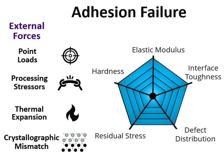
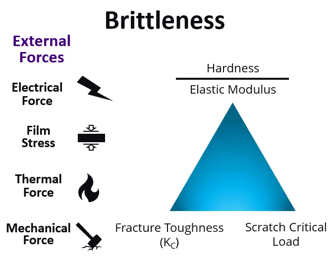
Semiconductor Film Adhesion Failure and Brittleness
Defect propagation, film and layer mechanics, and interface failure are contributing factors to the failure of semiconductor and compound semiconductor films. Adhesion failure occurs when external forces drive stress concentration at interfaces, where dissimilar materials meet. The brittleness of a material refers to the initiation and propagation of cracking within the material system. Common stressors that lead to brittle failures of semiconductor material systems include mismatched thermal expansion coefficients, electrical piezo forces, mechanical loading, and/or film stresses. Because of the likelihood that external factors and undetermined material properties may generate expensive latent defects later in the device manufacturing process or even later as field failures, the Nano Indenter G200X Semi Pack solutions provide new critical data to help reduce these failures and improve lifetime yields.
Semiconductor Failure Factor: Defect Propagation
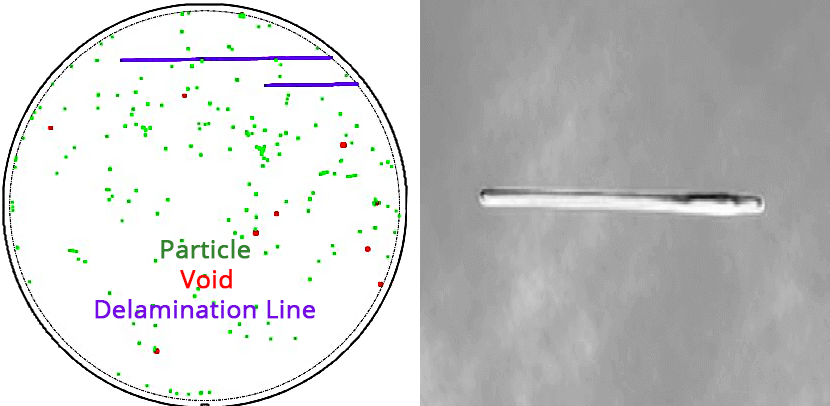
Problem: Existing flaws in substrates, films and layers are stress concentrators that easily propagate, exacerbating the failures that cause additional yield loss during fabrication and are prime locations for field failures. Micro pits, film steps, and delamination lines all are examples of stress concentrators.
Solution: KLA Instruments nanoindenters quantify the energy required to propagate a crack in film layers by measuring fracture toughness and cracking threshold; lower fracture toughness and cracking thresholds imply easier crack initiation and propagation. KLA is known for defect inspection and process control technology, and now KLA Instruments Nano Indenters generate a leap forward in the semiconductor industry to evaluate the likelihood that a defect will propagate during fabrication through fracture toughness, hardness testing and other methods.
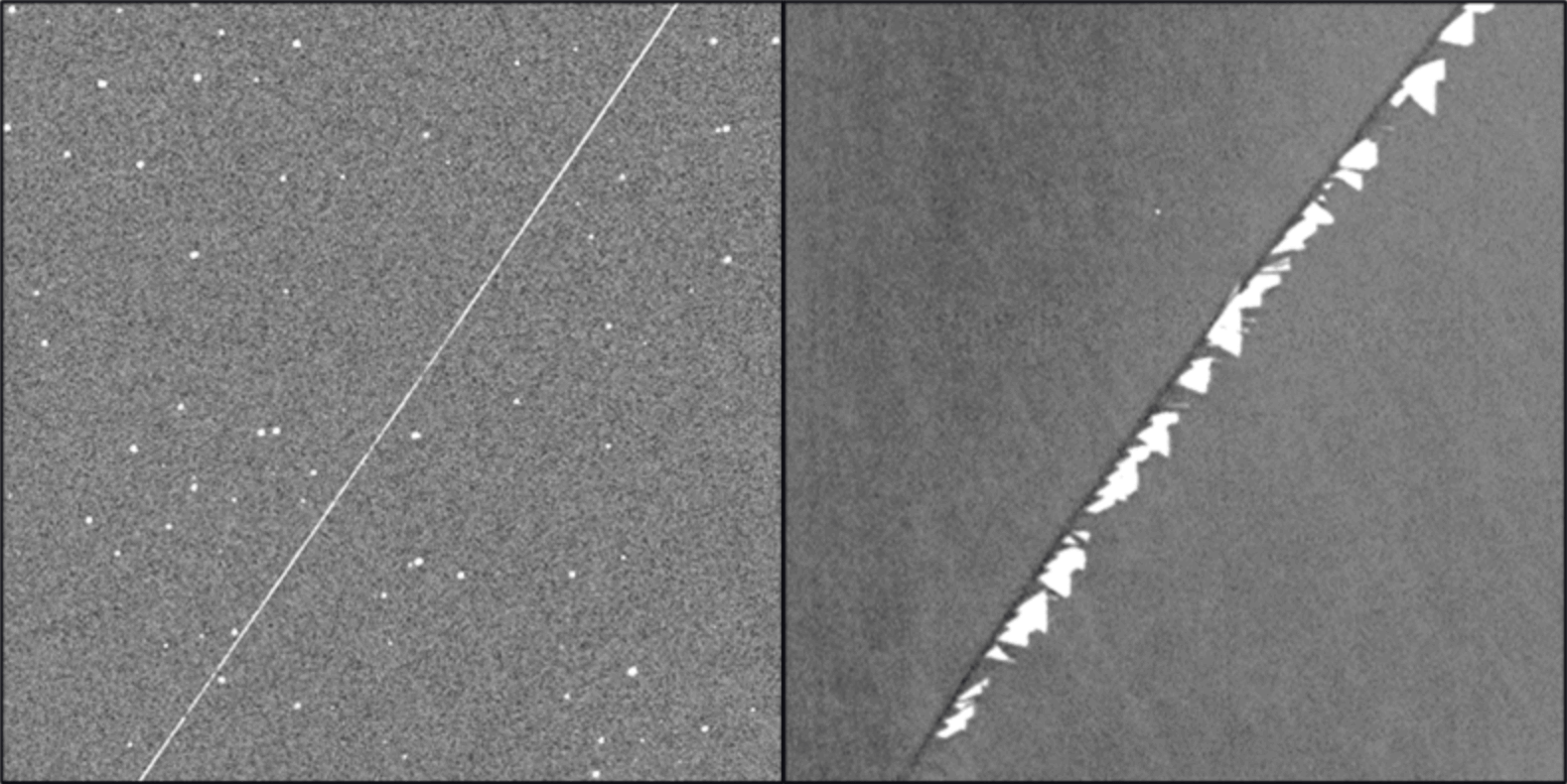
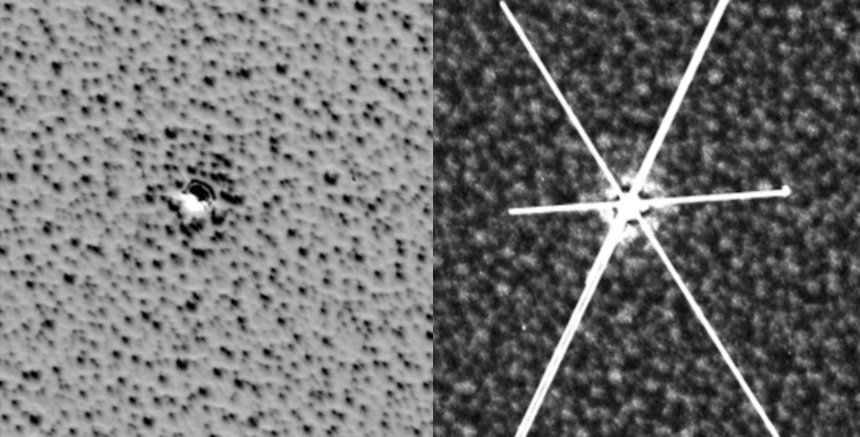
Semiconductor Failure Factor: Film and Layer Mechanics
Problem: Weak film layers allow stress migration, voiding, scratching and cracks, reducing yield and reliability.
Solution: KLA Instruments nanoindenters accurately measure mechanical properties to analyze processing effects in order to prevent failures. Surface hardness testing of films and mechanical properties measurement on CMP pads prevent scratches before they start. Measuring elastic modulus of dielectric films enables operators to prevent migration, which causes shorts and voids. These examples of surface analysis are only some of the information that KLA nanoindenters can bring to semiconductor failure analysis, failure prevention, and process control.
Semiconductor Failure Factor: Interface Failure
Problem: Weak interfaces caused by mismatched layer crystallography, thermal expansion coefficients and buffer layers lead to delamination adhesion failures. External point loads and mismatched expansion drive stress concentration to the interface of these layers, debonding them. Processing steps such as thermal processing, wire bonding and probe inspection cause interfacial stress concentration; each step is another opportunity for a latent defect to emerge and kill the device.
Solution: KLA Instruments nanoindenters provide the highest sensitivity in film adhesion testing to characterize and prevent delamination. Unlike other macro-scale tests such as four-point bend or Maszara adhesion testing, the nanoindenter provides localized analysis of delamination adhesion energy so that variations across the wafer can be quantified. This data provides feedback for optimizing buffer layer processing and monitoring any process variations that exacerbate delamination.
Download the G200X Semi Pack Option Sheet today to learn how nanoindentation data can improve yield and help prevent latent defects for your semiconductor or compound semiconductor devices.