Packaging Manufacturing
Packaging Manufacturing
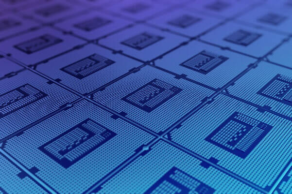
KLA’s extensive portfolio of packaging solutions accelerates the manufacturing process for outsourced semiconductor assembly and test (OSAT) providers, device manufacturers, foundries and IC substrate manufacturers for a wide range of packaging applications. Innovations in advanced packaging, such as 2.5D/3D IC integration using through silicon vias (TSVs), wafer-level chip scale packaging (WLCSP), fan-out wafer-level packaging (FOWLP) and heterogeneous integration as well as a wide range of IC substrates create new and evolving process requirements. KLA offers systems for a broad range of etch and deposition process solutions for advanced packaging applications, as well as packaging inspection, metrology, die sorting, chemistry process control, in situ process management and data analytics focused on meeting quality standards and increasing yield before and after singulation. KLA also provides a portfolio of technologies that includes automated optical inspection (AOI), automated optical shaping (AOS), direct imaging (DI), UV laser drilling, inkjet/additive printing and software solutions to ensure manufacture of the highest quality of IC substrates.