KLA’s new Axion® T2000 metrology system harnesses the power of X-rays to measure the complex vertical structures that form advanced memory chips.
With a wavelength much shorter than visible light, X-rays can pass through objects with little absorption, allowing them to “see” inside visually opaque or very thick objects without damaging them. These properties make X-rays useful for commonplace applications, such as medical diagnoses and airport security screening.
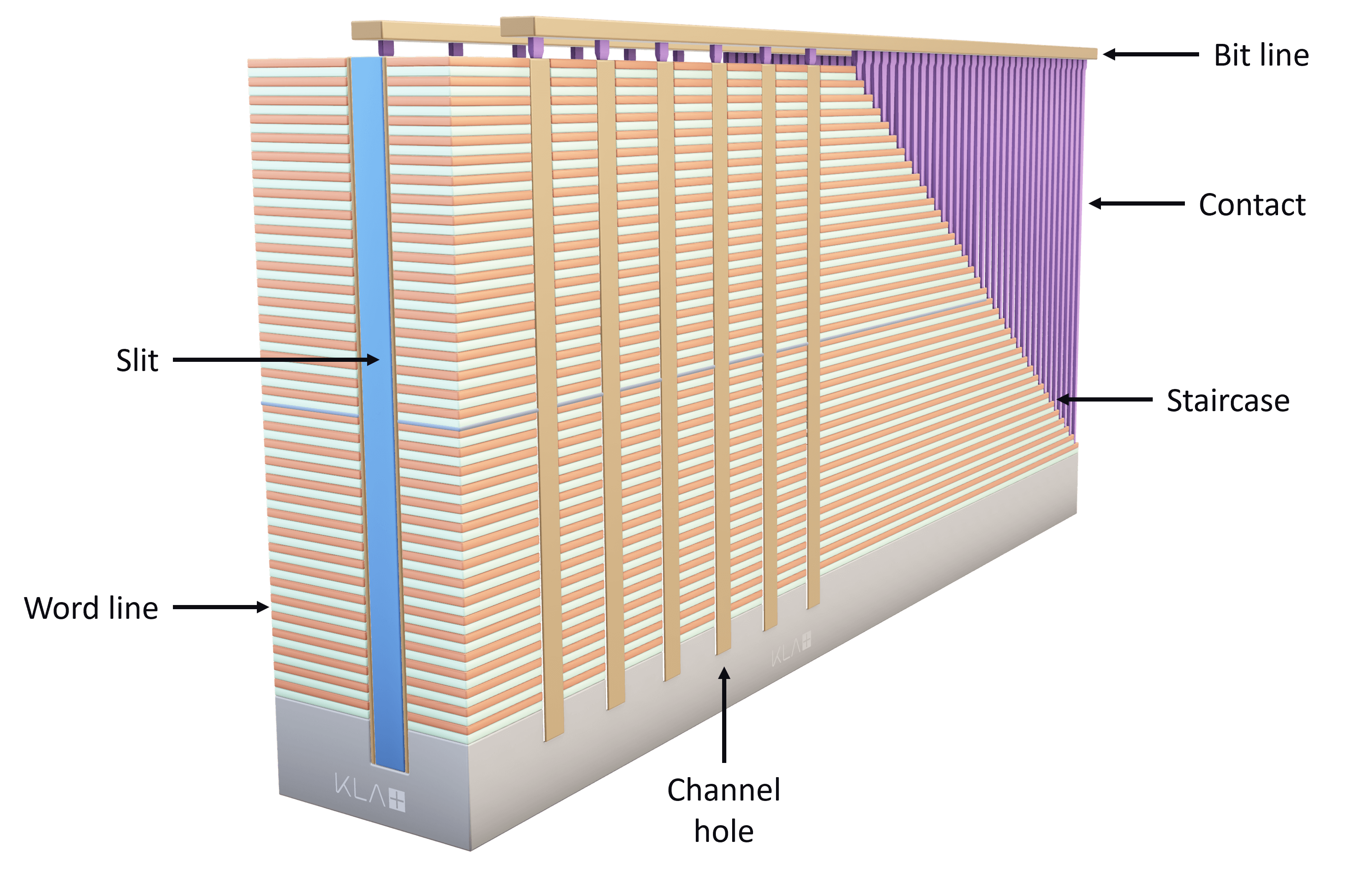
Likewise, X-rays are used for metrology applications in chip manufacturing, where it has become necessary to “see” inside vertical memory device architectures. Chipmakers have been leveraging innovations in vertical scaling to achieve memory chip performance gains, rather than solely relying on planar scaling. 3D NAND memory chips, for example, have grown taller and taller with each new generation – stacking cells to incredible heights to achieve improved chip performance within a compact device footprint.
The fabrication of these vertical memory chips involves the formation of high-aspect ratio (HAR) structures. These are nanoscale architectural features that are very tall and very narrow. For example, channel holes are formed by etching holes ~65-100nm in diameter into a film stack that is upwards of 10µm high and growing taller – resulting in an aspect ratio of ≥100:1. These HAR structures need to be formed with a near-perfect vertical shape profile, uniform from the top of the structure to the very bottom.
To understand if these vertical structures are being formed correctly, memory manufacturers need to precisely measure them along the entire height, and that’s where X-rays come in. X-rays pass through the memory device, collecting high-resolution shape information along the entire vertical dimension of the HAR structures. This is done without damaging the memory chip at a speed fast enough for inline monitoring of multiple process steps during high volume manufacturing.
A Unique X-Ray Metrology Solution
The Axion T2000 is a unique X-ray metrology solution for vertical memory chip manufacturing that uses CD-SAXS (critical dimension small angle X-ray scattering) technology. As shown in the animation below, a high flux source produces X-rays that travel through custom optics and then transmit through the wafer, which is mounted vertically in a stage. The X-rays interact with the memory device structures on the wafer, creating diffraction patterns that are imaged by a high-efficiency detector. The stage, with industry-leading dynamic range, precisely rotates the wafer so that the X-rays pass through at several different angles of incidence and azimuths. The resulting set of diffraction images is encoded with 3D geometrical information. KLA’s industry-leading AcuShape® modeling software extracts complex shape profile information from these images, including the subtle shape variations that can affect memory chip functionality or performance.

With its X-ray vision, the Axion T2000 provides high-resolution, non-destructive, critical dimension and 3D shape measurements, reducing the cycle time required to identify the most challenging shape variations in vertical memory chips. Examples of structural variations measured by the Axion T2000 include 3D NAND channel hole etch shape, tilt, bending and multi-tier overlay; and slit profile, bending and tungsten voids. The data produced by Axion is used by memory manufacturers during all stages of the fabrication process. During R&D, the Axion T2000 is used to achieve fast cycles of learning, reducing dependence on long lead time, destructive measurement methods such as FIB-SEM, TEM and cross-section SEM. It accelerates ramp cycle time by helping process engineers accurately characterize new processes, design nodes and devices. During high volume production, the Axion T2000 monitors key process steps inline to ensure variations that affect memory chip quality are identified and quickly addressed.
To learn more about KLA’s Axion T2000 X-ray metrology system, click on the product fact sheet (left) or visit the Axion product entry on KLA’s website.
Follow Us